
PN junction
When a p type semiconductor is suitably joined with n type semiconductor, a junction is formed called PN junction.
Depletion layer and potential barrier
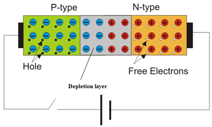
When p and n type materials are interfaced, the surface of contact of p and n type materials is called junction. In p-type material, holes are the majority carriers while in the n type material, the majority carriers are electrons. Due to electrons-hole recombination at the junction, the smaller region in the vicinity of the junction which has been depleted of free charge careers and has only immobile ions, which is called depletion layer. The p. d. developed across the depletion layer is called potential barrier.
Biasing of p-n junction diode
Biasing is defined as connecting external battery to the PN junction diode. A diode is said to be forward biased if p side is connected to positive terminal and n side is connected to negative terminal of a battery. Similarly, it is said to be reverse biased if p side is connected to negative terminal and n side is connected to positive terminal of a battery.
Characteristics of junction diode
Forward and reverse biased
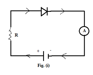
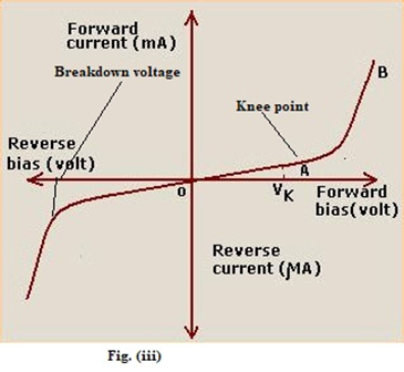
Consider, a circuit consisting of an adjustable DC voltage source in series with a resistor and diode as shown in figure 1. When the applied voltage is 0, there is no current. As we increase the voltage, electrons begin to flow. Because of series combination, the current is same in all parts of the circuit. This current increases slowly at first. When the applied voltage is approximately equal to the barrier potential, the current increases rapidly, such voltage is called knee voltage (Vk), as shown in figure (iii).
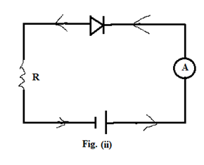
Figure (ii) shows reverse bias. If the applied voltage is zero, no current flows. When we increase the voltage, small current flows. When the reverse voltage is excessive, a few thermally produced free electrons carries high speeds. Once free, the valence electrons (Now free electrons) accelerate because of strong electric field and collide with other valence electrons. The process ends in an avalanche with huge number of valence electrons breaking from their orbitals and becoming free electrons. The voltage where avalanche occurs is called breakdown voltage (VB) as shown in figure (iii).
You've reached the end of the free preview. Continue with NN Premium.
- Complete access to every Premium chapter
- Notes, QBank, solutions & MCQs
- Premium PDFs & study resources
- Entrance preparation & mock tests
One NN Premium subscription unlocks everything.