
Solids
SYLLABUS
Energy bands in solids (qualitative ideas), Difference between metals, insulators and semi-conductors using band theory, Intrinsic and extrinsic semi-conductors
What is This Chapter About?
Look around you — the chair you sit on, the screen you read from, the wire carrying electricity to your device, the semiconductor chip inside your phone. All of these are solid materials, and yet they behave in dramatically different ways. Some conduct electricity freely, others block it completely, and some — the most technologically important of all — do a little of both under controlled conditions. Why do these differences exist? The answer lies not in the chemical composition of these materials alone but in the quantum mechanical structure of their electrons — specifically, in the way energy levels in individual atoms broaden into energy bands when billions of atoms come together to form a solid.
Chapter 25 of NEB Grade 11 Physics introduces the band theory of solids — one of the most successful applications of quantum mechanics to real materials. It explains the electrical behaviour of metals, insulators, and semiconductors from first principles and introduces the concepts of intrinsic and extrinsic semiconductors that are the foundation of all modern electronics. Carrying 3 teaching hours as a concise but conceptually rich chapter, it directly connects quantum physics to the technological world.
Key Concepts You Will Learn
From Energy Levels to Energy Bands
In an isolated atom, electrons occupy discrete, well-defined energy levels — the quantum states described by Bohr’s model and its quantum mechanical refinements. When atoms are brought together to form a solid, something remarkable happens. The electrons of neighbouring atoms interact with each other, and by the Pauli exclusion principle (no two electrons can occupy exactly the same quantum state), the discrete energy levels split and broaden into continuous ranges of allowed energies called energy bands.
Each energy band consists of an enormous number of very closely spaced energy levels — so close that they effectively form a continuum within the band. Between adjacent bands are energy gaps (or band gaps) — ranges of energy that no electron in the solid can have.
The two most important bands for understanding electrical conductivity are the valence band — the highest band that is completely or partially filled with electrons at absolute zero — and the conduction band — the next higher band, which may be empty, partially filled, or separated from the valence band by a gap.
Metals, Insulators, and Semiconductors — Band Theory Classification
The electrical behaviour of a material is determined entirely by the band structure at the Fermi level and the size of the band gap.
Metals (conductors) have either a partially filled conduction band or an overlapping valence and conduction band. In either case, there are electrons already in the conduction band that can move freely under an applied electric field — this is why metals conduct electricity so easily. Copper, aluminium, gold, and iron are metallic conductors. There is no energy gap between valence and conduction bands.
Insulators have a completely filled valence band separated from the empty conduction band by a very large energy gap — typically 5 eV or more. At room temperature, thermal energy (about 0.025 eV at 300 K) is far too small to excite electrons across this gap. No electrons reach the conduction band, so no current flows. Diamond (band gap ~5.5 eV) and silicon dioxide (band gap ~9 eV) are insulators.
Semiconductors have a band structure similar to insulators but with a much smaller energy gap — typically 0.1 to 2 eV. At absolute zero, semiconductors behave like insulators. At room temperature, thermal energy is sufficient to excite a small but significant number of electrons across the gap into the conduction band, leaving behind holes (vacancies) in the valence band. Both the conduction electrons and the holes can carry current — this is why semiconductors conduct electricity to a moderate degree. Silicon (band gap 1.1 eV) and germanium (band gap 0.67 eV) are the most important semiconductor materials.
Intrinsic Semiconductors
A pure semiconductor with no impurities is called an intrinsic semiconductor. In an intrinsic semiconductor, every electron promoted to the conduction band leaves behind exactly one hole in the valence band — the number of conduction electrons equals the number of holes:
[latex]n_e = n_h = n_i[/latex]
where [latex]n_i[/latex] is the intrinsic carrier concentration. Both electrons (moving in the conduction band) and holes (moving in the valence band in the direction opposite to electron motion) contribute to electrical conduction.
The conductivity of an intrinsic semiconductor increases strongly with temperature — as temperature rises, more electrons gain enough energy to cross the band gap, increasing the carrier concentration. This is the opposite behaviour from metals (which become more resistive at higher temperatures due to increased lattice vibrations). The temperature dependence of semiconductor conductivity is the basis of the thermistor — a temperature sensor whose resistance changes dramatically with temperature.
Extrinsic Semiconductors
The electrical properties of semiconductors can be dramatically modified by introducing tiny amounts of impurity atoms — a process called doping. The resulting material is called an extrinsic semiconductor.
n-type semiconductors are formed by doping silicon (which has 4 valence electrons) with a pentavalent impurity — an atom with 5 valence electrons — such as phosphorus, arsenic, or antimony. Each impurity atom forms 4 covalent bonds with neighbouring silicon atoms, with one extra electron left over. This extra electron is only weakly bound (the binding energy is much smaller than the band gap) and can easily be promoted to the conduction band at room temperature, contributing to conduction. The impurity atoms are called donors (they donate electrons to the conduction band). In n-type material, electrons are the majority carriers and holes are the minority carriers.
p-type semiconductors are formed by doping silicon with a trivalent impurity — an atom with 3 valence electrons — such as boron, aluminium, or gallium. Each impurity atom forms only 3 covalent bonds with neighbouring silicon atoms, leaving one bond incomplete — a hole that can accept an electron from the valence band. These impurity atoms are called acceptors (they accept electrons from the valence band, creating holes). In p-type material, holes are the majority carriers and electrons are the minority carriers.
Doping is extraordinarily powerful — adding just one phosphorus atom per million silicon atoms increases the conductivity of silicon by a factor of about 10,000 at room temperature. This precise control of conductivity through doping is the foundation of all semiconductor device technology.
Why This Chapter Matters for NEB Exams
Solids is examined consistently in NEB Grade 11 Physics. The distinction between energy levels (in isolated atoms) and energy bands (in solids) — explaining why bands form — is a standard short-answer question. Classifying metals, insulators, and semiconductors using band theory — drawing band diagrams with valence band, conduction band, and band gap — is a classic examination question. The definitions of intrinsic and extrinsic semiconductors, and the distinction between n-type (donor impurities, electron majority carriers) and p-type (acceptor impurities, hole majority carriers) are examined as both conceptual questions and drawing/labelling questions. The relationship between band gap size and electrical behaviour is a frequent conceptual question.
Important Topics to Focus On
- How isolated atomic energy levels broaden into energy bands in solids
- Energy band diagram — valence band, conduction band, band gap, Fermi level
- Metals — partially filled conduction band or overlapping bands, free electrons
- Insulators — large band gap (>5 eV), no electrons in conduction band at room temperature
- Semiconductors — small band gap (0.1–2 eV), some electrons thermally excited at room temperature
- Comparison table: metals, insulators, semiconductors — band gap, conductivity, temperature dependence
- Intrinsic semiconductor — pure material, equal electron and hole concentrations
- Holes as charge carriers in the valence band
- Extrinsic semiconductor — doped material
- n-type — pentavalent donor impurity, electrons are majority carriers
- p-type — trivalent acceptor impurity, holes are majority carriers
- Effect of temperature on intrinsic semiconductor conductivity
- Application: thermistor (temperature-dependent resistance)
- Numerical problems on band gap energy, carrier concentrations, and conductivity
Connection to Other Chapters
Solids builds on Grade 12 Chapter 23 (Quantization of Energy) — energy levels in atoms are the precursors of energy bands in solids, and the Pauli exclusion principle determines how electrons fill these levels. It connects directly forward to Grade 12 Chapter 22 (Semiconductor Devices) — the p-n junction, diode, and logic gates are all built from the n-type and p-type semiconductors introduced here. The thermistor introduced in this chapter reappears in Grade 11 Chapter 23 (DC Circuits) as a sensor in potential divider circuits. The band gap energy connects to Chapter 21 (Photons) — a photon with energy greater than the band gap can excite an electron across the gap (the basis of solar cells and photodetectors), while an electron falling back across the gap emits a photon (the basis of LEDs and semiconductor lasers). The temperature dependence of semiconductor conductivity connects to Grade 11 Chapter 9 (Heat and Temperature) through the Boltzmann factor governing the number of thermally excited electrons.
i. Crystalline Solids:
The solids in which the atoms, molecules and ions, which constitutes the solids are arranged in definite pattern in 3D, is called crystalline solids. They have homogeneous composition, have sharp melting and boiling points. The bonds in the solids are strong. E.g. rock salt, sugar, etc.
ii. Amorphous Solids:
The solids in which atoms, molecules and ions are not arranged in regular symmetrical patterns are called amorphous solids. Their composition may not be homogeneous. They do not have sharp melting and boiling points. Example ordinary glass, Sulphur, plastics, etc.
Energy band:
The range of energy possessed by an electron in a solid is known as energy band. There are various energy bands:
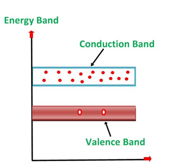
i. Valence band:
The outermost electrons present in the outermost shell of an atom is called valence electrons. The range of energy possessed by these valence electrons is known as valence band.
ii. Conduction band:
At ordinary temperature, valence electrons have tendency to leave valence band. And these valence electrons are responsible for the conduction of current in a conductor and so they are called conduction electrons. The range of energy possessed by the conduction electrons are called conduction band.
iii. Forbidden energy gap or band gap ([latex]E_g[/latex]):
The separation between top of the valence band and bottom of the conduction band is called forbidden energy band or band gap. On the basis of band theory, metal, insulator and semiconductor are distinguished.
You've reached the end of the free preview. Continue with NN Premium.
- Complete access to every Premium chapter
- Notes, QBank, solutions & MCQs
- Premium PDFs & study resources
- Entrance preparation & mock tests
One NN Premium subscription unlocks everything.